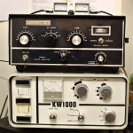
I’ve been keying my KW1000 linear using a relay to buffer the FT847. The FT847 closed a 12V circuit across the relay and the relay in turn keyed whatever voltage/current the linear requires. The relay in the KW1000 is old, large and whilst it had been modified from the original circuit, I still don’t have confidence with it being within the limits of the 847.
All was well until a flyback diode I placed across the ‘buffer’ relay to protect the 847 failed short. This resulted in the 847 keying 12V @ 1A ultimately limited by my bench PSU. The surface mount 847 PTT transistor promptly cooked itself.
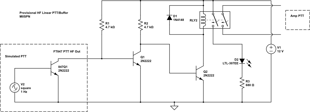
I now plan to redesign the PTT interface including additional transistors to protect the radio. My planned schematic is below:-
The box to the left is my simulated 847. The 847 closes the HF STBY pin to ground on TX. In the above design R1 now limits the current seen by the 847 to 12/4700=~3mA. By default Q1 is biased ‘on’ by R1, pulling the collector to ground, resulting in Q2 switched ‘off’ and the relay unactivated.
When the 847 keys the PTT line, the base of Q1 is pulled to ground, the emitter then floats to a positive voltage (>0.6V) and Q2 switches ‘on’. This allows current to flow from Q2’s emitter->collector and the relay energises.
Flyback diode D1 protects the transistor from reverse EMF generated from the relay coil. Only this time, if D1 fails short it’s Q2 that becomes toast, not the microscopic surface mount transistor in a £700 radio.
Both Q1 and Q2 are set to draw about 3mA across their base-emitter junctions. Assuming an Hfe of 100, in the case of Q2 this should be more than enough to allow 120mA across emitter-collector (assuming relay coil is 100ohm). In the case of Q1 it’s probably overkill; I wonder what the benefit is of lowering this besides power consumption?
Note: Circuit designed for 100ohm relay coil resistance whereas I believe the actual relay at hand is 720 ohm (so 20mA); current plot above has been updated to reflect this.
Any comments appreciated.
Edit: 16.06.15
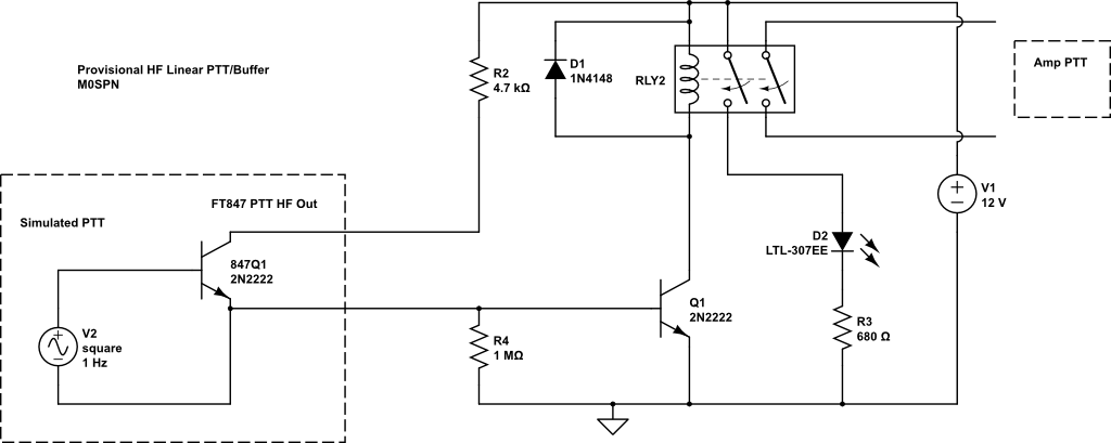
As always, I seem to miss the simple things. Rather than the FT847 radio pulling the first transistor low (requiring a second transistor to invert the output), the PTT could directly pull the second transistor high, simplifying the design and losing a transistor.
However, my original quest was to not only isolate the radio and linear but provide additional protection against the flyback diode failing short. In the above scenario, should D1 fail in this way, Q1 would probably quickly follow. The radio would only be protected until this point, depending on exact mode of Q1 failure.
The original two-transistor schematic seems to offer an additional layer of protection. In this case, should Q2 also fail short, Q1 would be outside the path of destructive current flow.
For this reason, I intend to continue with construction and testing of the first (v1) schematic.


Pingback: Swan 1200X and KW1000 | M0SPN
Hi, using a 90 mA relay wich type of transistors ?
Thank you, 73